Die analysis of the 8087 math coprocessor's fast bit shifter (2020)
Die Analysis: The 8087 Math Coprocessor's Fast Bit Shifter (2020)
Based on the research by Ken Shirriff
While floating-point arithmetic is indispensable for scientific computing, early microprocessors were limited to direct integer support. Although mainframes in the 1950s and '60s handled floating-point numbers, it wasn't until 1980 that Intel released the 8087 floating-point coprocessor for the microcomputer market.
Integrating this chip into a system like the IBM PC provided a massive performance boost, making floating-point calculations faster. This was a game-changer for software such as:
- Flight simulators
- Spreadsheets
- AutoCAD
The Challenge of Precision
Implementing floating-point operations is notoriously difficult due to the need for extreme accuracy and speed. Engineers must account for:
Simple additionComplex rounding and overflow handling.- Edge cases and transcendental operations.
Before the 8087, floating-point implementations were fragmented and incompatible. Intel solved this by collaborating with William Kahan, a numerical analysis expert, to build a system based on rigorous mathematical principles.
The resulting architecture became the IEEE 754 standard, which is still utilized by nearly every modern computer today, cementing the 8087's legacy as one of the most influential chips ever created.
Hardware Breakdown
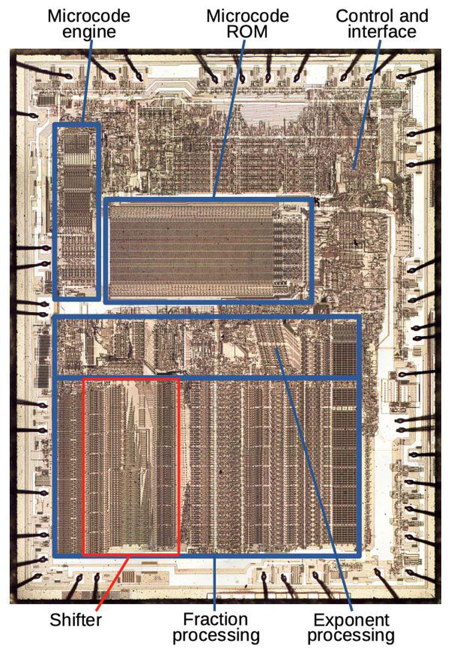
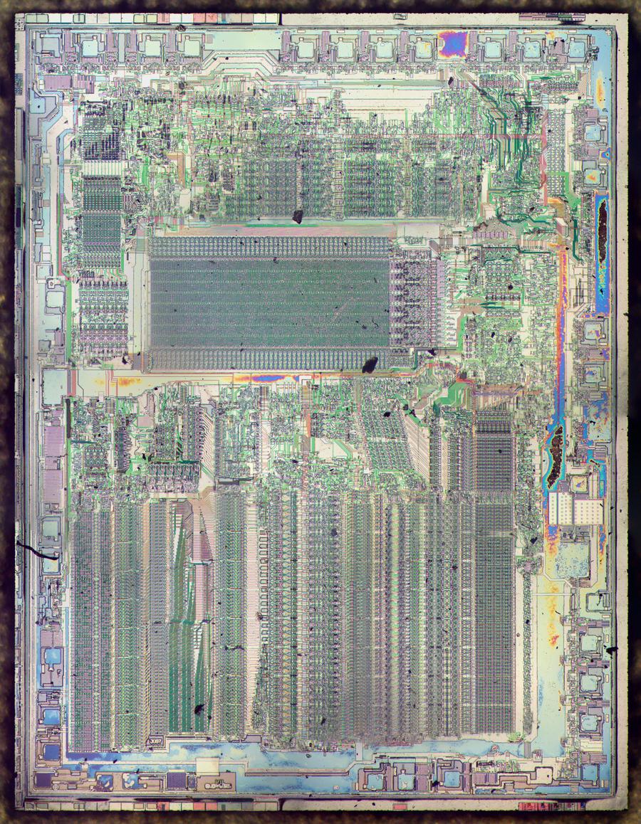
To understand the inner workings, the 8087 was decapped and examined via microscopy. The chip was a marvel of its time, pushing the limits of fabrication.
| Component | Transistor Count |
|---|---|
| Intel 8086 (CPU) | 29,000 |
| Intel 8087 (FPU) | 40,000 |
Functional Layout
A floating-point number is composed of three primary elements:
- Sign bit
- Exponent
- Fraction (also known as the mantissa or significand)
(Where is the fraction and is the exponent)
The chip's physical layout reflects these components:
- Bottom Section: Fraction processing (includes a constant ROM, the shifter, adder/subtracters, and the register stack).
- Middle Section: Exponent processing circuitry.
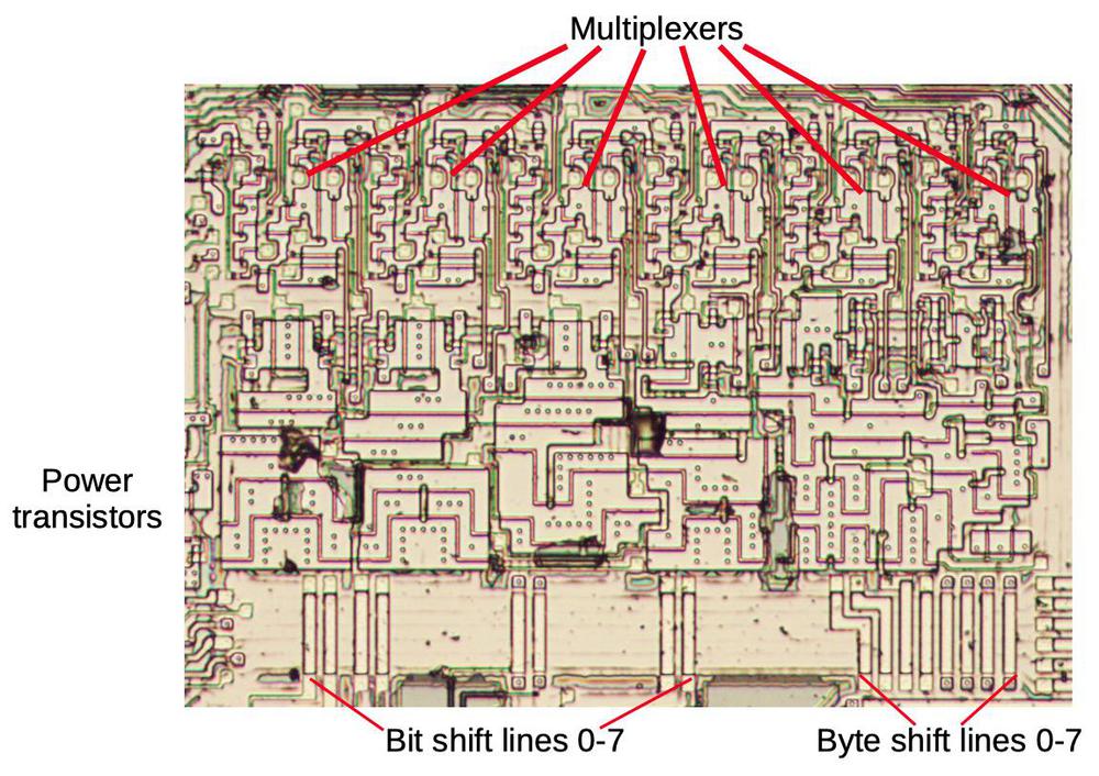
The High-Speed Shifter
The shifter is a massive component on the die because it is critical for several operations:
- Alignment: Shifting binary points to line up numbers for addition/subtraction.
- Transcendentals: Powering the
CORDICalgorithm via shift-and-add sequences. - Assembly: Combining 16-bit memory chunks into a full floating-point number.
The Barrel Shifter Architecture
To avoid the slowness of shifting one bit at a time, Intel implemented a barrel shifter. This allows a value to be shifted by any number of positions in a single clock cycle. To keep the area manageable, they used a two-stage design:
By combining these, the 8087 can shift a value by any amount from 0 to 63 bits.
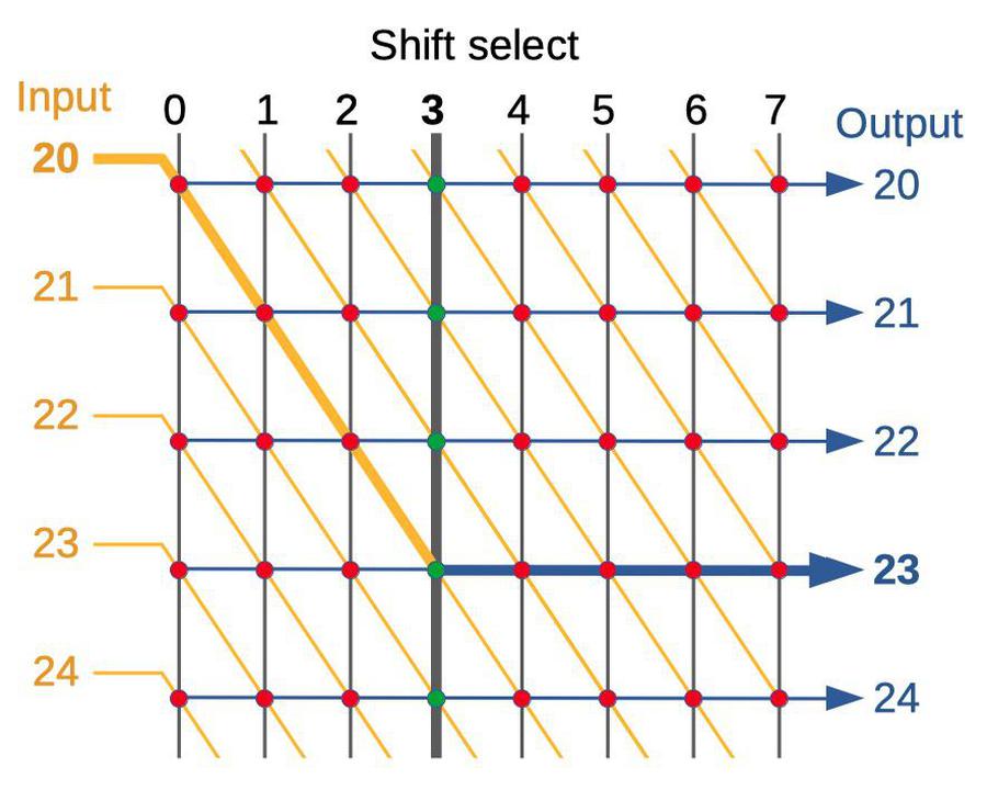
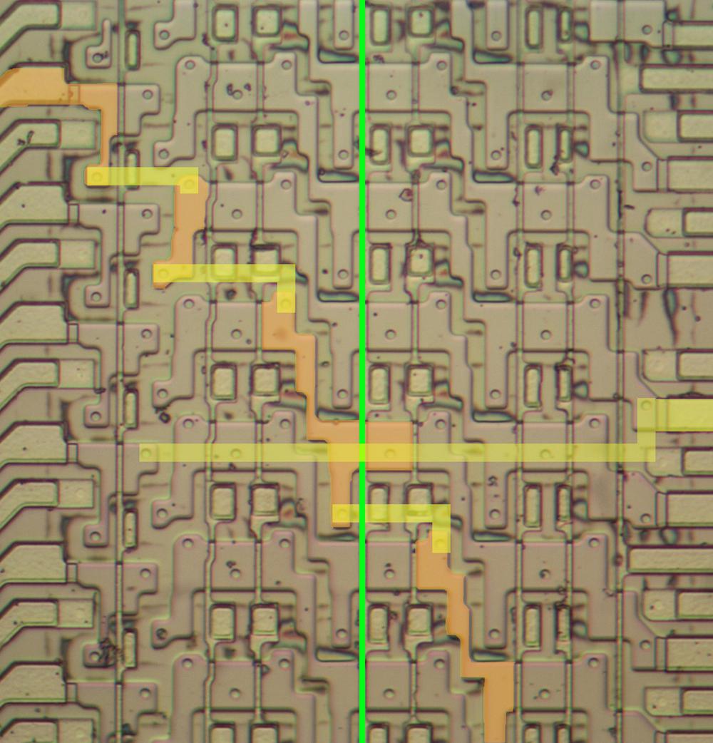
Deep Dive: The Bit Shifter
The first stage handles shifts of 0 to 7 positions. While the full shifter supports 68 bits, the logic follows a specific matrix pattern:
- Input Lines: Run horizontally.
- Select Lines: Run vertically to activate specific columns of transistors.
- Transistors: Act as switches connecting an input to an output.
- Diagonal Routing: Each input connects to eight different transistors diagonally.
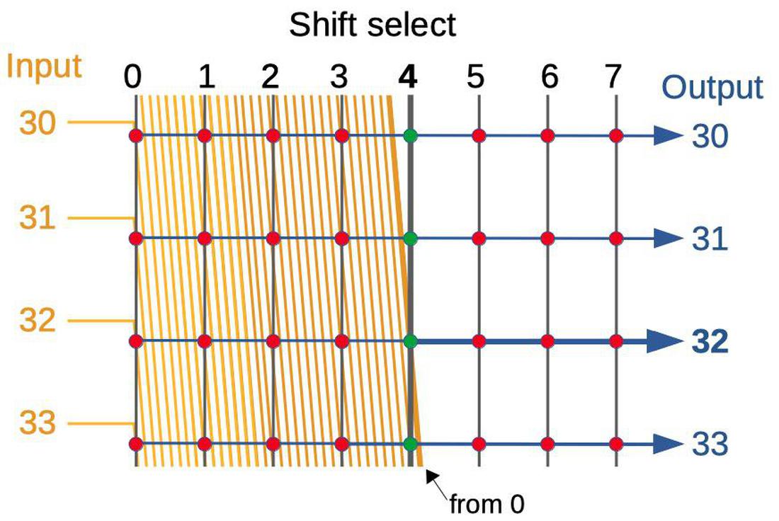
Example Scenario:
If shift select line 3 is energized:
- The transistors in that column activate.
Input 20is routed toOutput 23.- This results in a net shift of 3 bits.
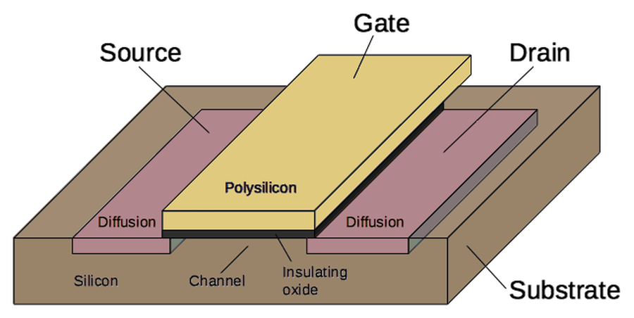
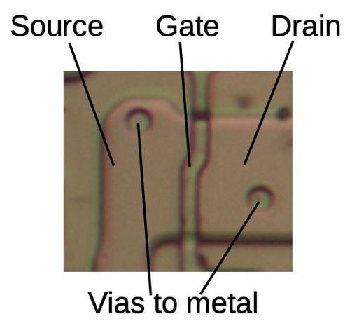
Silicon Implementation (NMOS)
The 8087 utilizes NMOS transistors. These are created by doping the silicon substrate to create "diffusion" regions.
The MOSFET Structure
A transistor functions as a switch controlling current between two points:
- Source & Drain: The two regions the current flows between.
- Gate: A layer of polysilicon above the substrate.
When voltage is applied to the gate, the path between the source and drain opens. These transistors are then interconnected using a metal layer on top of the chip.
Microscopic View
Under a microscope, the transistors appear as complex shapes. The metal wiring is connected to the silicon via circular holes called vias. In the provided analysis photos, the metal layer was removed using acid to reveal the underlying NMOS structure.
In a small section of the bit shifter, approximately 48 of these transistors can be seen working in tandem to route signals.
// Conceptual logic of the shifter select
if (select_line == 3) {
    output[i + 3] = input[i];
}
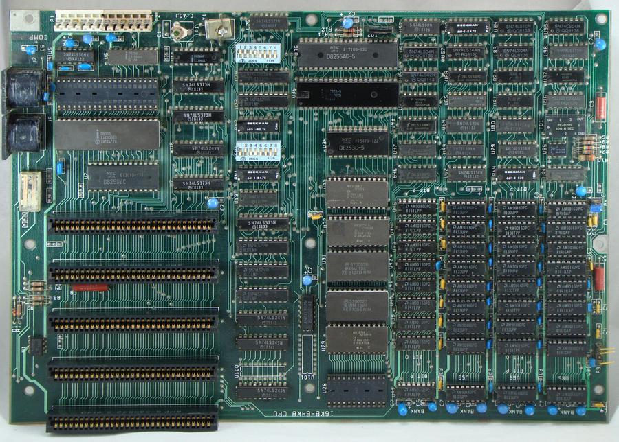
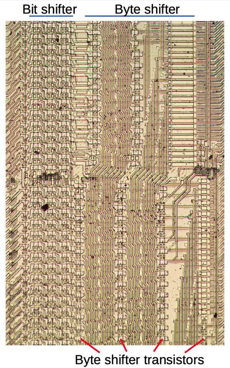
Additional Die Imagery
- Byte Shifter Structure:
- Combined Shifters:
- Decoder Circuitry:
- Stripped Die:
- Context: