Advanced Nintendo Entertainment System (ANES) – NES Modded to Use 2 PPUs
Advanced Nintendo Entertainment System (ANES)
Enhancing the NES with Dual PPU Architecture
The ANES project is a hardware modification designed to push the graphical boundaries of the original Nintendo Entertainment System by integrating two Picture Processing Units (PPUs) instead of one.
Author's Note: I don't expect many people to actually undertake this build, so please be aware that the documentation may be somewhat incomplete or "half-assed" in certain areas.
If you prefer a software-based approach over soldering, you can experiment with this concept via a modified fork of the Mesen2 emulator.
🛠️ Hardware Requirements
To execute this mod, you will need components from both your primary console and a donor unit. The following table outlines the necessary Bill of Materials (BOM):
| Qty | Location | Part Number | Description |
|---|---|---|---|
| 2 | U1, U2 | RP2C02 | PPUs (harvested from two consoles) |
| 1 | U3 | AS6C6264-55PCN | Static RAM dedicated to PPU2 |
| 1 | U4 | 74LS373 | Address latch (from donor) |
| 1 | U5 | 74LS139 | Demultiplexer (from donor) |
| 1 | U1 | EMS-26405 | 40-pin wire wrap socket for PPU1 |
| 2 | J1 | — | 20-pin female pin headers |
| 1 | U5/J3 | — | 16-pin socket for the 74LS139 |
| 4 | RN1 | 1/4 watt EXT pull-down resistors | |
| 1 | — | 6x8cm board | Prototype board |
| 1 | U2 | — | 40-pin socket for PPU2 (Optional) |
| 1 | U3 | — | 28-pin socket for RAM (Optional) |
| 1 | U4 | — | 20-pin socket for latch (Optional) |
🏗️ Build Process
The assembly can be broken down into the following sequence of operations:
- Prepare the Prototype Board: The standard 6x8cm board is
perfectly sizedslightly too large and will block the expansion port. Trim it down before proceeding. - Component Harvesting: Desolder the
RP2C02(U5) from both your target console and the donor console. - Clear Space: Relocate or fold down capacitors that obstruct the placement of the dual-PPU board.
- Header Installation: Solder the two 20-pin female headers into the original PPU footprint.
- Board Assembly: Construct the dual-PPU board using the provided KiCad schematics and reference photos.
- Demultiplexer Modification:
- Take a 16-pin IC socket and remove pins
6, 7, 9, 10, 11, 12, 13, 14, and 15. - Mount this socket over the console's existing
74LS139, soldering only pins1, 8, and 16. - Create the following jumper connections:
- Socket Pin 2 CPU Address Line
A12 - Socket Pin 3 Console
74LS139Pin 5 - Socket Pins 4 & 5
/CEpins of PPU1 and PPU2 respectively.
- Socket Pin 2 CPU Address Line
- Take a 16-pin IC socket and remove pins
- Final Integration: Plug the completed dual-PPU board into the female headers.
Logic Flow of PPU Selection
🖼️ Visual References
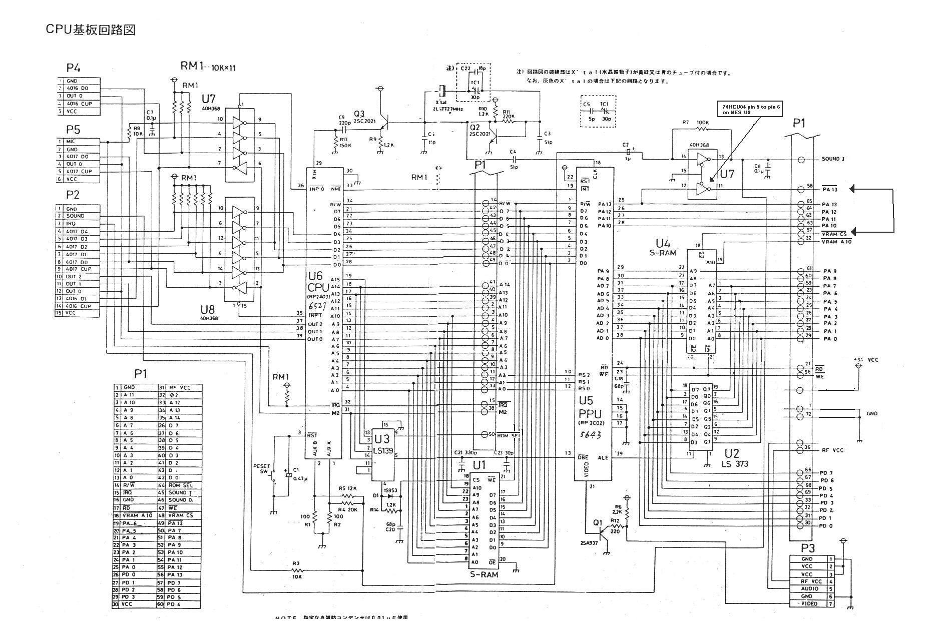
Schematics & Layouts:

Hardware Placement:


Modding the Demultiplexer & Caps:


🔗 Related Resources
If you want to see this hardware in action or test the logic via software, check out these repositories:
- Emulator: Mesen2 Fork
- Demos:
📜 License
This project is released under the following license:
GPL-3.0 License