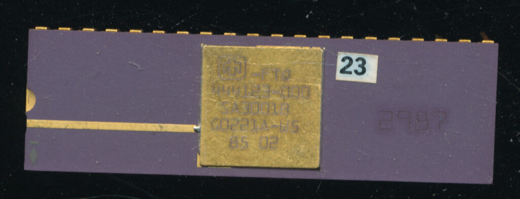
Sandia National Labs SA3000 8085 CPU
Sandia National Labs SA3000 8085 CPU


This article is featured in the CPU Shack Museum, a massive archive boasting over 20,000 CPUs, 150+ manufacturers, and 2,000+ EPROMs. The museum offers a wide array of test boards for sale, ranging from the MCS-4/40 and RCA COSMAC to Intel i3002 and Motorola 68060 systems.
The Genesis of Sandia's Fabrication Capabilities
During the transition from the late 1970s into the early 1980s, the Sandia National Laboratory in Albuquerque, New Mexico, established its own internal capacity to design, fabricate, and test integrated circuits (ICs) on a large scale. While Sandia handled the internal logic and fab, the final packaging was outsourced to Allied Signal and Fairchild.
Why a National Lab?
The primary driver for this investment was the requirement for radiation-hardened (rad-hard) electronics. These components were essential for:
- Space Exploration: Missions facing extreme cosmic radiation.
- Defense Systems: Specifically nuclear warheads, ICBMs, and reentry vehicles.
Fabrication Evolution
The facility's technical capabilities grew rapidly over a few years:
| Year | Wafer Size | Process Node | Notable Application |
|---|---|---|---|
| 1978 | Initial capacity building | ||
| 1982 | Galileo Space Probe (Jupiter Mission) |
For the Galileo probe, Sandia took existing logic diagrams for processors and support chips and rebuilt them using their specialized rad-hard process, producing over 50,000 units for the probe, testing, and backups.

The SA3000: A Rad-Hard 8085
In 1982, Sandia embarked on a project to convert the Intel 8085 (originally an HMOS design) into a radiation-hardened CMOS version, designated as the SA3000.
Technical Specifications
Converting the architecture to CMOS was a complex task, resulting in a device containing approximately 18,000 transistors. One of the most difficult hurdles was the instruction decoder—a large Programmable Logic Array (PLA) that is straightforward in NMOS but challenging in CMOS.
# SA3000 Hardware Profile
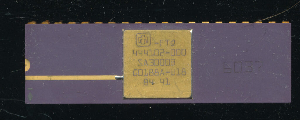
Die_Size: 228-239 mils
Operating_Voltage: 4.5V to 11V
Testing_Compatibility: 5V
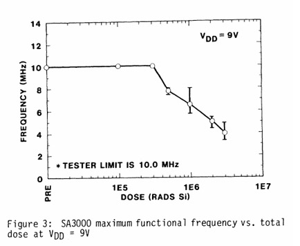
Max_Clock_Speed: 10MHz
Manufacture_Date: 1984 (Lot G Wafer 18)
Design Note: The ability to operate up to provided critical "headroom." Because radiation exposure typically degrades the maximum speed of a device, the higher voltage allowed the chip to maintain functionality even as it slowed down.
The Support Ecosystem
The SA3000 didn't work alone; Sandia created a suite of compatible rad-hard support chips:
SA3001based on Intel 8155SA3002based on Intel 8355SA3026based on Intel 8212
The Art of Radiation Hardening
Achieving reliability in the harshest environments required a blend of science and art. Sandia employed several specific fabrication techniques:
- Substrate Choice: Used an epitaxial substrate to prevent latchup.
- Isolation: Implemented extensive guard rings around transistors.
- Oxide Strength: Hardened the oxides by strictly controlling production temperatures.
- Grounding: Maximized the frequency of power-to-substrate and ground-to-guardband/p-well contacts.
Performance Metrics
The SA3000 vastly outperformed its original design goals:
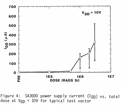
- Original Goal: rads.
- Actual Result A: rads (with only a performance loss).
- Actual Result B: rads (with a performance loss).
Deployment and Applications
The SA3000 found its way into some of the most critical hardware in US history:
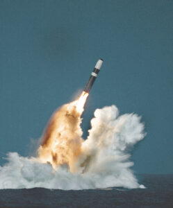
- W88 Nuclear Warhead: Used in the Trident II submarine-launched missile. Up to eight SA3000 CPUs manage the programmer for fuzing and altitude calculations.
- Deep Space Star Tracker: Developed by Ball Aerospace.
- CRRES (1990): The Combined Release and Radiation Effects Satellite used the chip to study electronics in high-radiation zones.
The mission was a total successThe electronics survived, but the battery failed after one year, ending the mission early.
Commercialization and Transition
Around 1984-1985, the US government transitioned the management of the fab to a contractor, Allied Signal. This move was unpopular with Sandia management and led to a decrease in operational efficiency, as Allied Signal lacked prior experience in fab management.
The Harris Era
By 1990, the SA3000 and its companions were commercialized by Harris under new part numbers.
Comparison: SA3000 vs. Harris Versions
| Feature | Sandia SA3000 | Harris HS1/HS9 |
|---|---|---|
| Voltage | Fixed | |
| Max Speed | ||
| Process | Same Rad-Hard CMOS | Same Rad-Hard CMOS |