Looking inside a 1970s PROM chip that stores data in microscopic fuses (2019)
Exploring the Architecture of a 1970s PROM Chip
In a fascinating dive into computer history, Ken Shirriff examined the MMI 5300, a memory chip from the early 1970s. This device is a PROM (Programmable Read-Only Memory), which differs from standard RAM in one fundamental way: it can be rewritten it is programmed exactly once. Once the internal fuses are "blown," the data is permanent.
At the time of its release, this chip—produced by Monolithic Memories Incorporated—carried a price tag of $70.
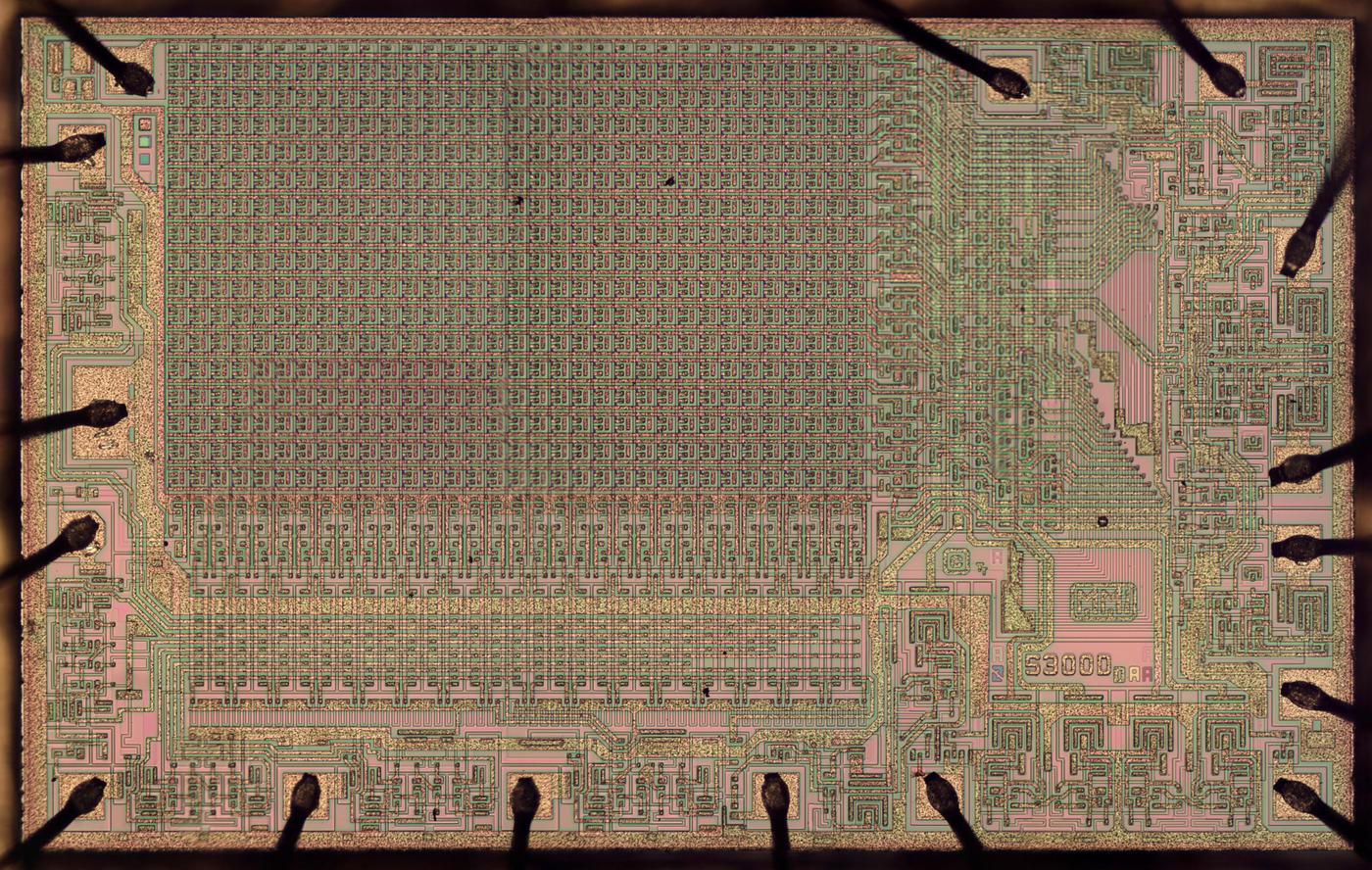
Physical Composition and Decapping
The MMI 5300 stores bits of data. Unlike the MOS transistors found in modern semiconductors, this chip utilizes NPN transistors.
To get a look at the internals, the process involved:
- Acquire 16-pin ceramic packages (MMI 5300 or 6300).
- Use a chisel to knock off the metal lid.
- Expose the silicon die and its bond wires.
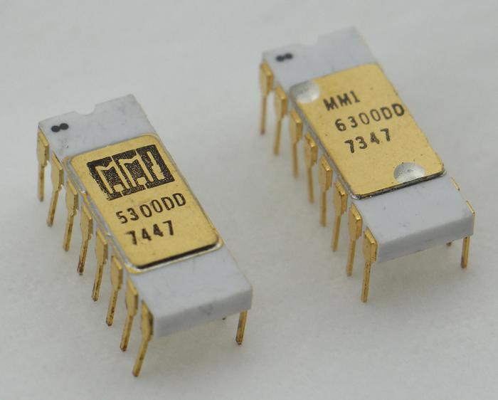
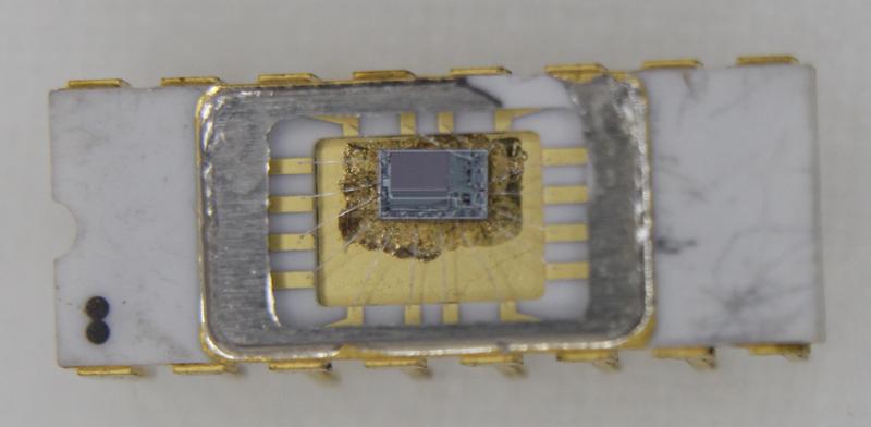
The die features a top metal layer for wiring, with silicon-based resistors and transistors residing underneath. Sixteen bond wires connect the die to the external pins.
Internal Architecture
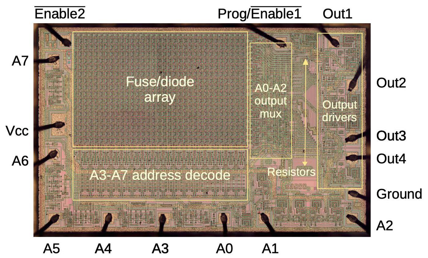
The chip's layout is divided between the data storage array and the supporting logic. While the data array occupies only about 25% of the total die area, it is the heart of the device.
Pin Configuration and Logic Flow
The following table summarizes the primary pin functions:
| Pin Group | Label | Function |
|---|---|---|
| Address | A0 - A7 | Selects one of 256 words |
| Output | Out1 - Out4 | Outputs the 4 bits of the selected word |
| Control | Program | Used to apply high voltage for blowing fuses |
The Memory Array
The bits are organized as 256 words of 4 bits each. However, for spatial efficiency, they are physically arranged in a square grid.
Addressing Logic:
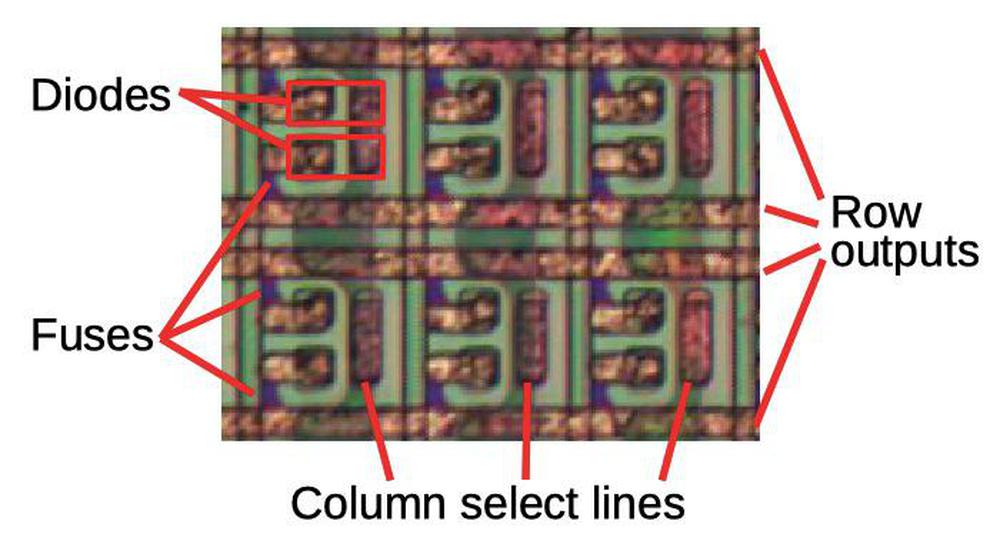
- Column Selection: Using 32 NAND gates (built with multiple-emitter transistors), address bits
A3-A7activate a specific column. - Row Selection: DTL multiplexers then use
A0-A2to narrow the 32 rows down to the 4 specific bits required for output.
The Physics of Data Storage
Data is stored using a combination of diodes and Nichrome fuses.
Note on Nichrome: This is a nickel-chromium alloy. Because it has significantly higher resistance than standard metals, it generates heat when current passes through it—the same principle used in household toasters.
Binary Representation
The logic state of a bit is determined by the physical state of the fuse:
- Intact Fuse Logic
1 - Blown Fuse Logic
0
Because the chip ships with all fuses intact, it begins as a sea of 1s. The user then "programs" the chip by selectively destroying the fuses where a 0 is needed.
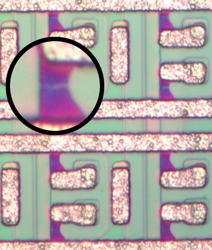
Interestingly, the fuses do not vaporize completely. Instead, they develop a microscopic crack approximately wide. Since this is roughly the wavelength of red light, the damage is just barely visible under a microscope.
The Programming Process
Programming the MMI 5300 required precision and high voltage, far exceeding the standard TTL levels.
The sequence for blowing a fuse:
- Select the target address.
- Apply to the
Programpin. - After a specific delay, apply to the desired output pin for a few microseconds.
This process had to be meticulously timed to ensure the Nichrome fuse melted without destroying the surrounding circuitry.
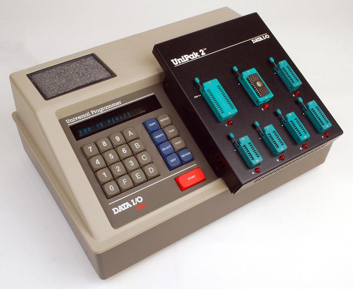
To automate this, engineers used expensive PROM programmers (costing around \6,000$) equipped with various sockets for different chip sizes.
Technical Detail: Transistor Construction
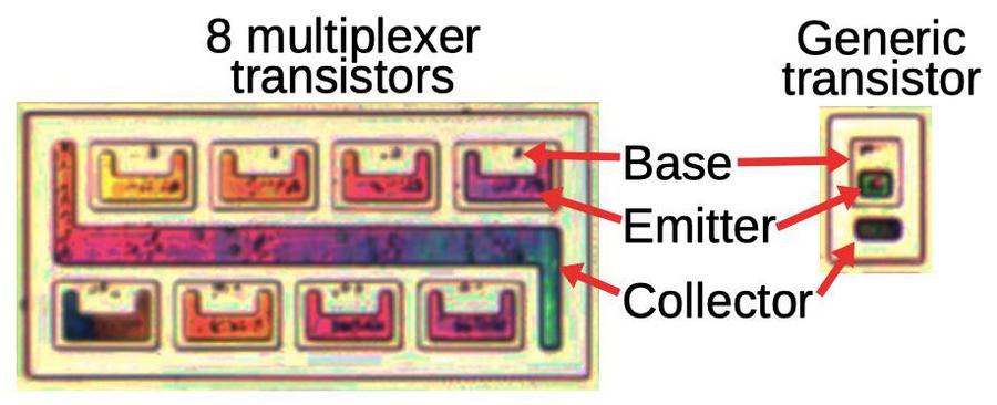
The multiplexers utilized specialized transistors. When the metal layer is removed, the N-doped silicon appears darker, and the remaining oxide creates a distinct colored appearance.
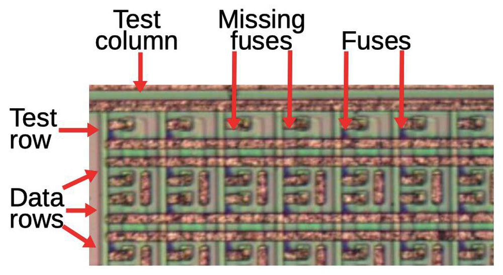
Finally, the chip included a small amount of redundancy:
Extra Row/Column Used for Factory Testing
// Conceptual logic of a PROM read
if (fuse_is_intact(address)) {
    return BIT_1;
} else {
    return BIT_0;
}