Hot Chips 2026: Samsung and HBM Base Die Opportunities
Hot Chips 2026: Samsung and HBM Base Die Opportunities
 By Chester Lam

The relentless appetite of machine learning workloads for massive memory bandwidth and capacity has forced a rethink of hardware architecture. Samsung's latest strategy involves a fundamental shift: fabricating HBM base dies on a logic node rather than a traditional DRAM node.
Understanding the HBM Architecture
High Bandwidth Memory (HBM) functions by stacking several DRAM dies vertically atop a single base die. These layers communicate via Through-Silicon Vias (TSVs), while the base die handles the communication with the compute die (GPU/CPU) through an interposer.
To increase bandwidth in newer generations, engineers must scale the throughput in two places:
- Between the DRAM layers and the base die.
- Between the base die and the host compute die.
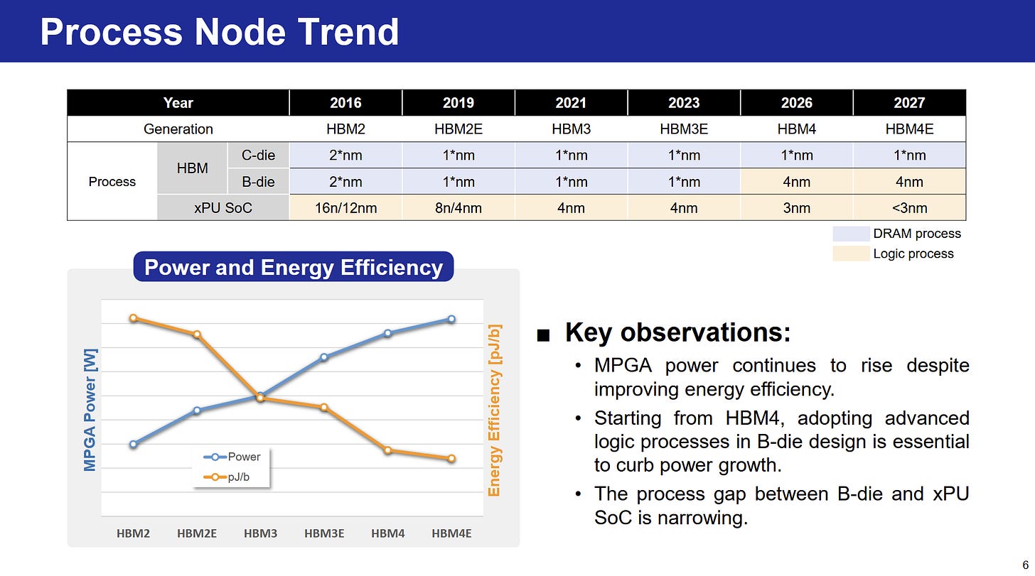
The second point is the bottleneck. The physical interface (the PHY) consumes the majority of the base die's real estate. Adding more data pins increases the footprint and spikes power consumption. While efficiency improves per generation, the total power draw continues to climb:
The Strategic Pivot: DRAM Node Logic Node
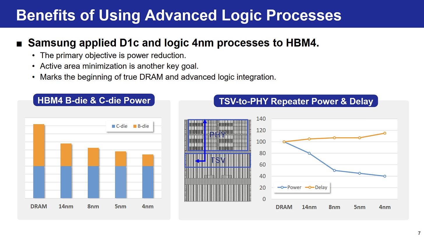
Samsung has addressed these constraints by switching the base die to a logic node.
| Feature | DRAM Node (Old) | Logic Node (New) |
|---|---|---|
| Power Consumption | Higher | Lower |
| Transistor Density | Lower | Higher |
| Area Efficiency | Limited | Optimized |
| Flexibility | Rigid | High (allows "extra" features) |
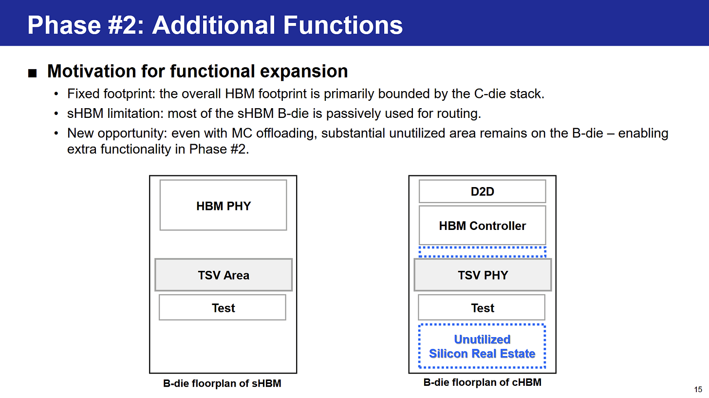
Because the base die's physical dimensions are fixed by the DRAM stack above it, moving to a denser logic node creates a surprising amount of unused silicon area. Samsung is now utilizing this "free" space across three distinct phases.
Phase 1: Intelligence at the Base
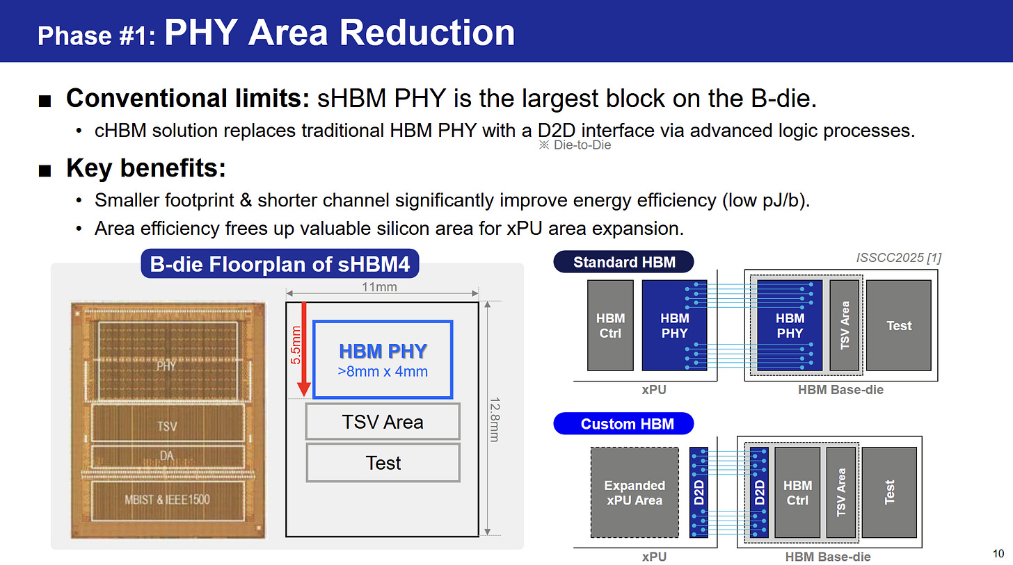
The primary goal of Phase 1 is to reduce power and optimize the interface.
- Integrate Memory Controller: Traditionally, DRAM is
"dumb"passive. The host compute die must manage low-level tasks like:- Precharging rows.
- Switching the bus between read/write modes.
- Refreshing cells.
- Custom Die-to-Die Interface: By moving the controller to the base die, Samsung can replace the standard HBM interface with a custom protocol. This reduces the
PHYarea on both the compute die and the base die.
Hypothetical Application: Imagine a processor similar to Intel's Sapphire Rapids, but where the HBM dies natively understand the CPU's internal mesh protocol.
The Trade-off: This approach increases integration complexity. Since it deviates from standard HBM protocols, Samsung may need to lead an industry effort to standardize this custom interface.
Advanced Error Correction
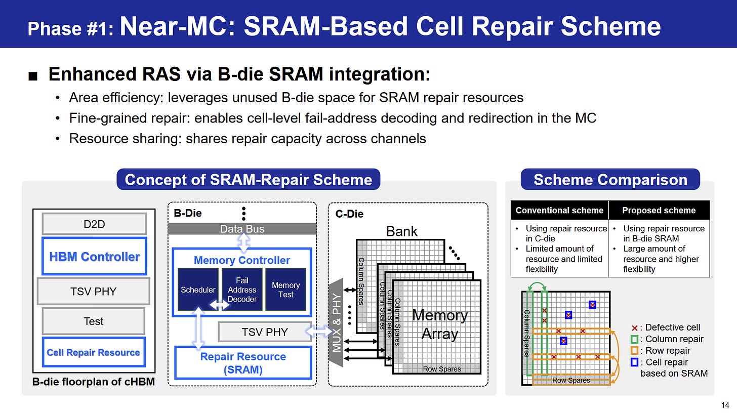
Samsung is also adding an SRAM block to the base die for remapping.
- Old Way: Row/column spares were limited to the specific die they were on.
- New Way: A centralized SRAM table allows any spare cell (even on a different die in the stack) to replace a defective one, greatly increasing flexibility.
Phase 2: Expanding Functionality
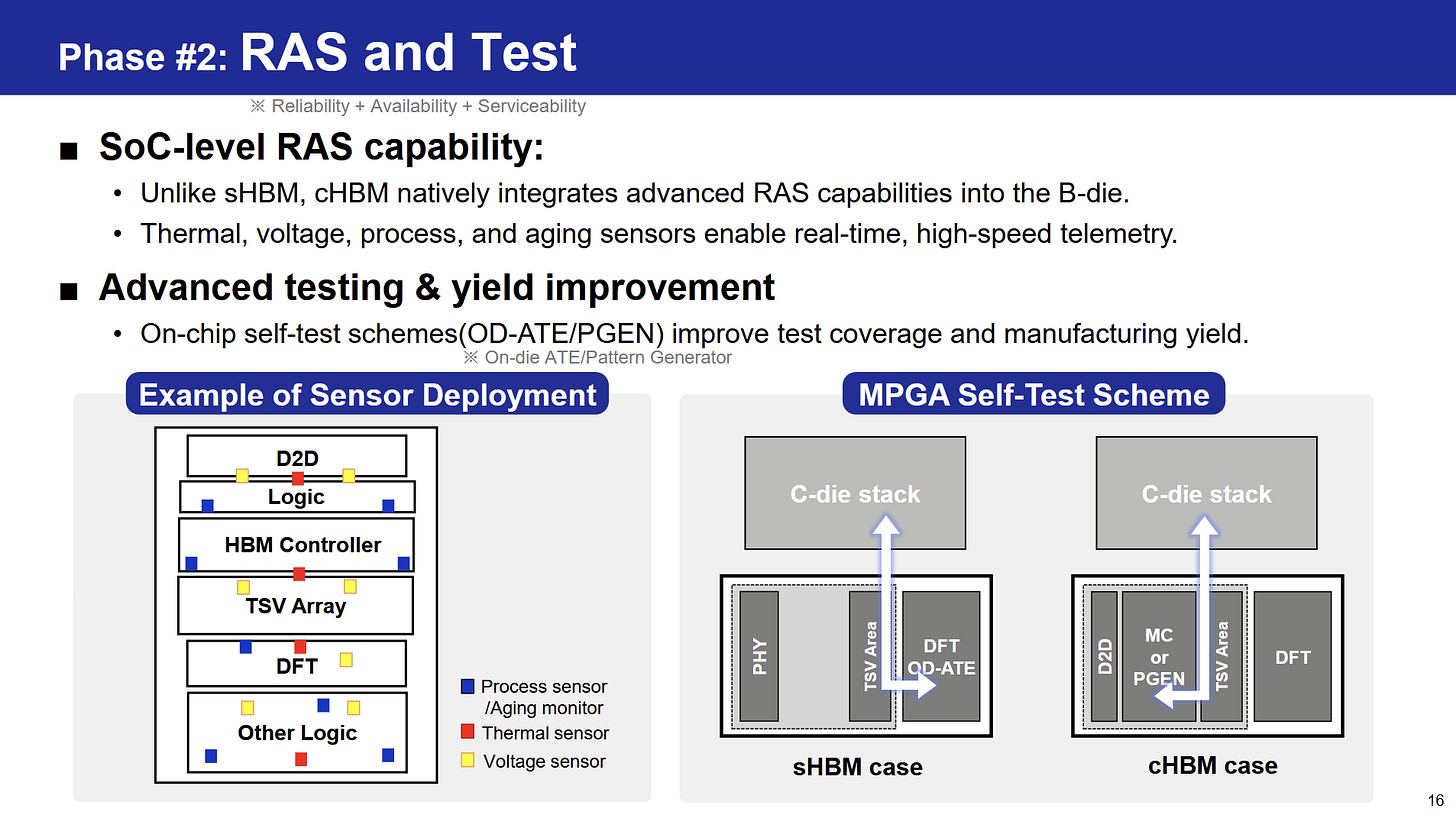
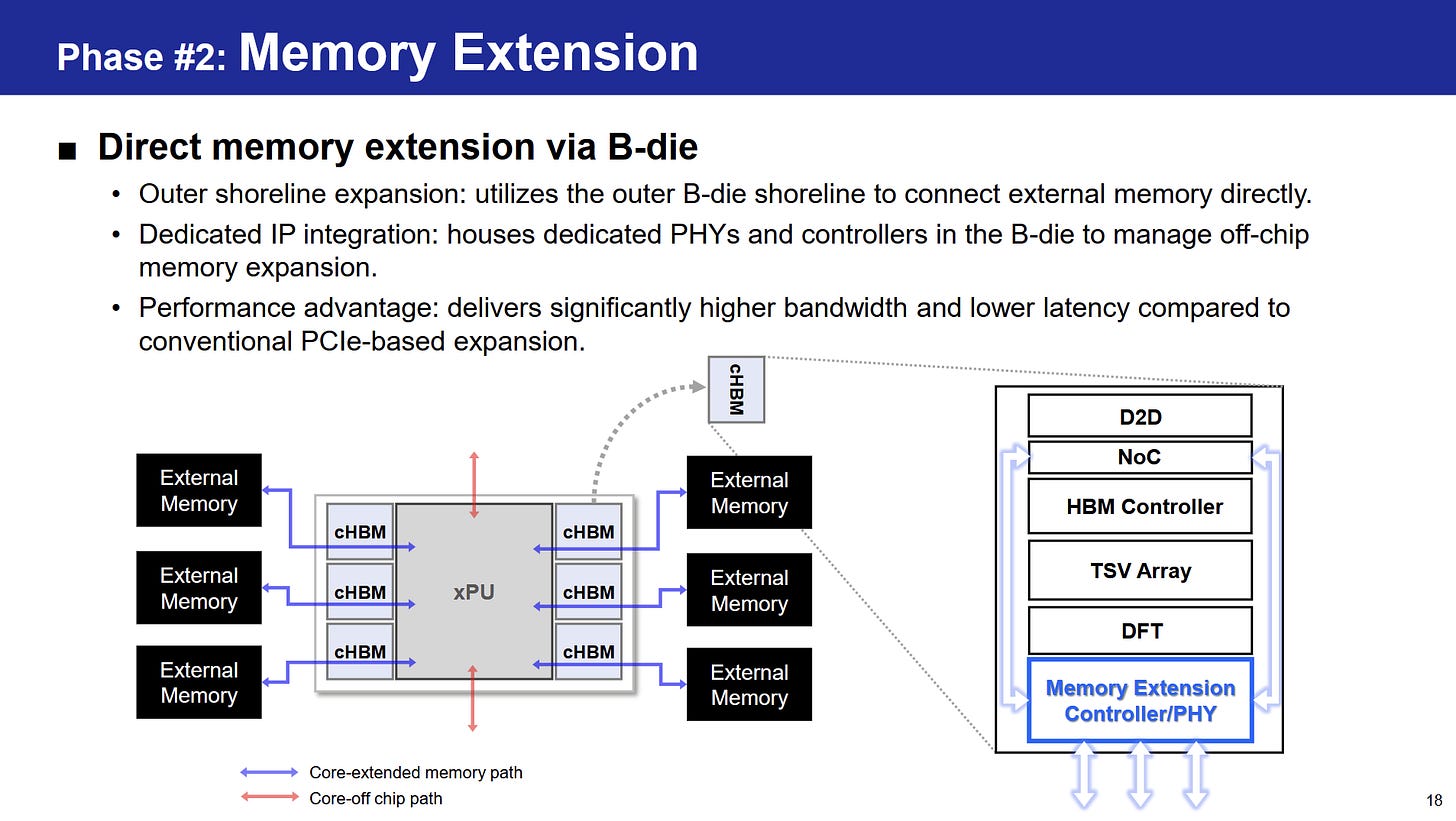
Even with a memory controller, Samsung found they still had spare room. Phase 2 focuses on telemetry and expanded I/O.
- Enhanced Telemetry: Integration of more sensors for real-time voltage and temperature monitoring.
- On-Die Testing: A dedicated test block that generates patterns (similar to
memtest) without requiring the host CPU. - External Memory PHYs: To bypass interposer size limits, the base die can act as an I/O hub, connecting the compute die to additional external memory.
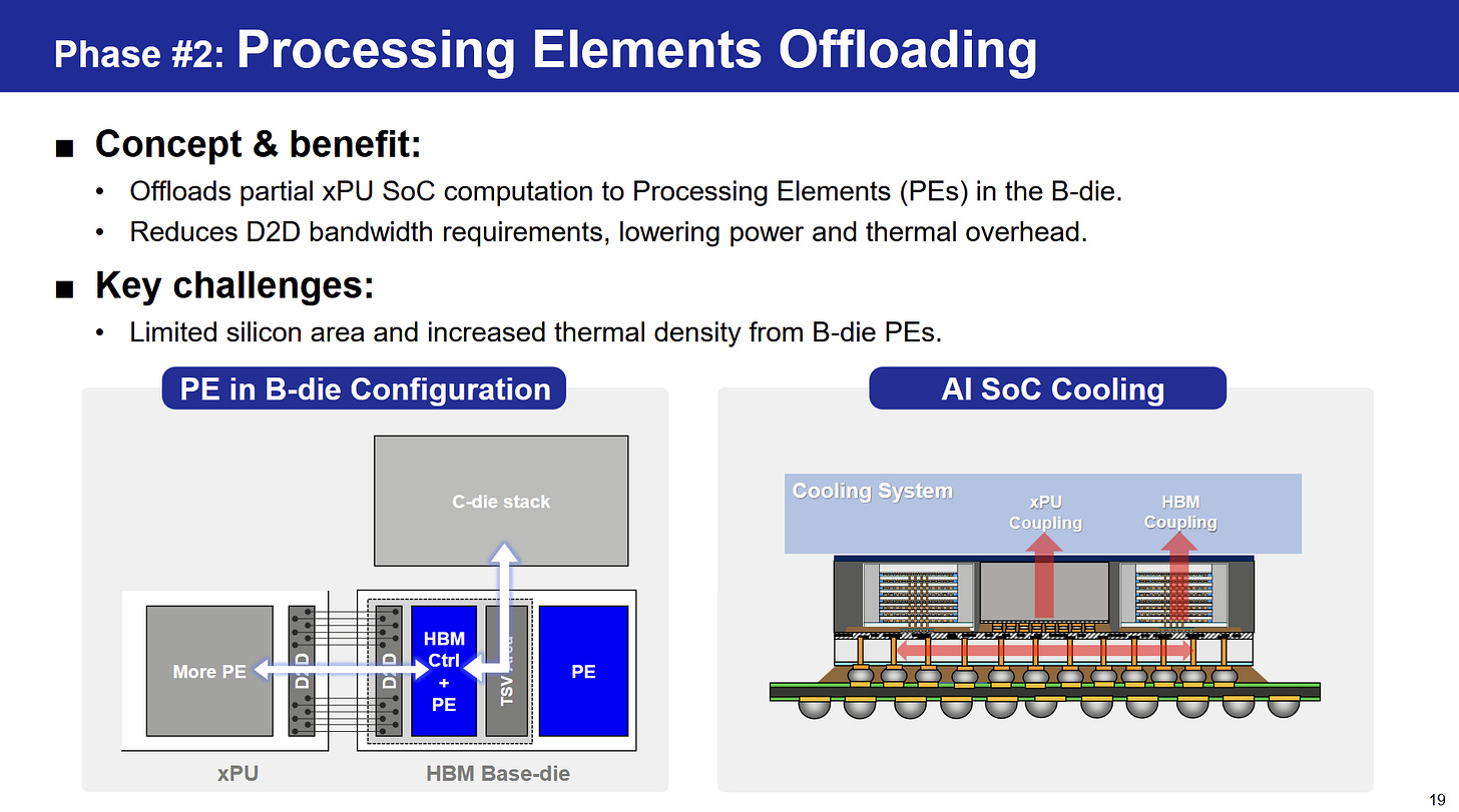
- In-Memory Compute: Performing basic operations directly on the base die.
A Note on Near-Memory Compute
The author expresses skepticism regarding general-purpose compute on the base die due to NUMA (Non-Uniform Memory Access) issues. Without large caches, processing units (PEs) would struggle with data homed on other dies. However, it remains highly viable for pre-processing, such as:
Input Data Format Conversion (Base Die) Compute Die
Phase 3: zHBM and 3D Stacking
The final frontier is zHBM, where the entire HBM stack is placed directly on top of the compute chip, similar to mobile Package-on-Package (PoP) designs.
The Thermal Challenge: Stacking memory creates a massive thermal blanket. We have seen this with AMD's 3D V-Cache (Zen 3, 4, and 5), where stacked variants often require lower clock speeds than non-stacked versions to manage heat.
If Samsung can solve the cooling equation, zHBM would allow:
- Maximum Area Savings: More room for compute cores.
- Minimum Latency: The shortest possible physical path between data and logic.
Final Thoughts
Samsung's roadmap represents a move toward an incredibly tight coupling between memory and compute. While technically promising, the biggest hurdle is ecosystem adoption. If chip designers want to source HBM from multiple vendors to avoid lock-in, Samsung must convince its competitors to adopt these custom logic-node solutions.