Samsung's Processing-in-Memory (PIM)
Samsung's Processing-in-Memory (PIM)
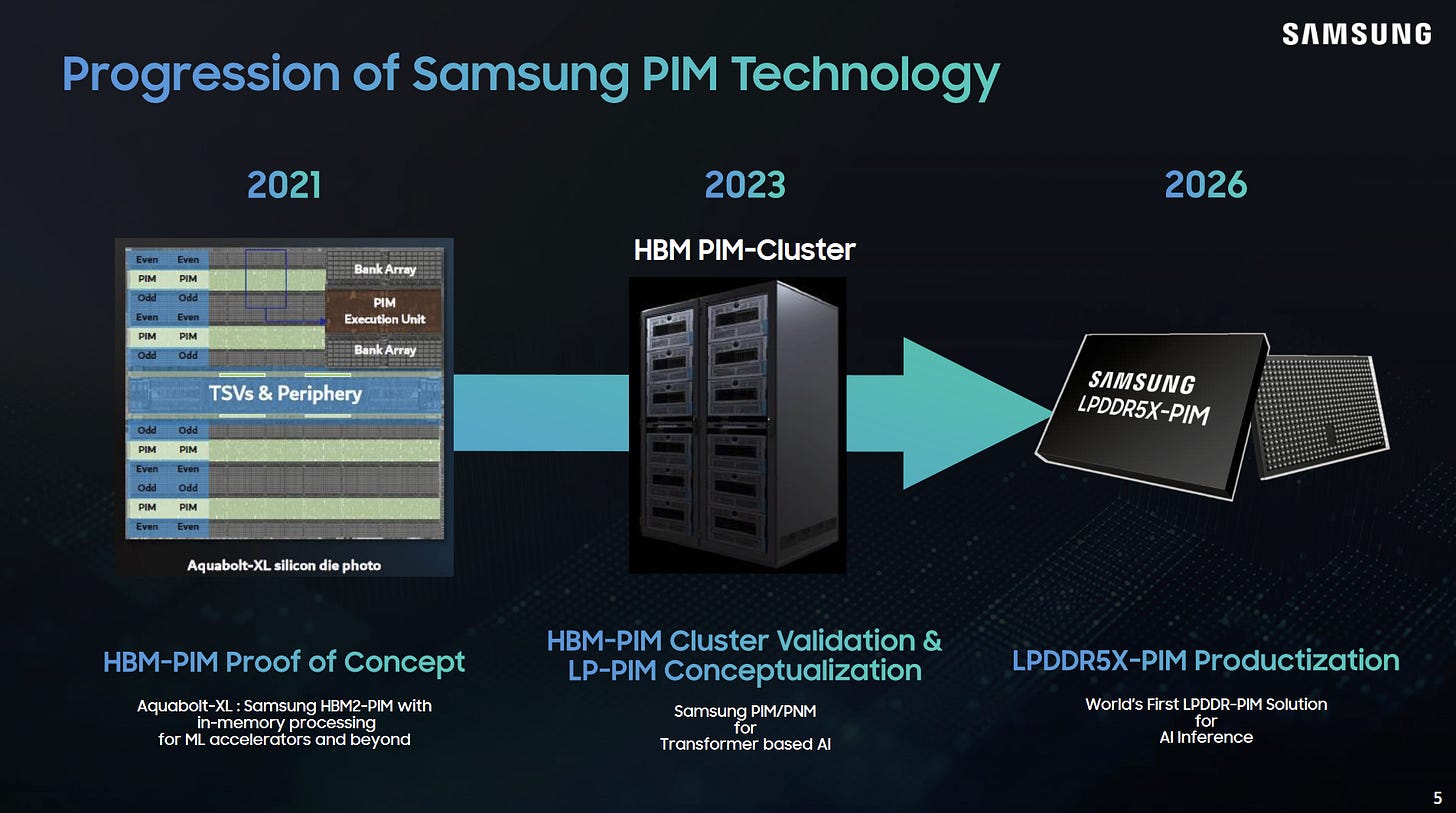
Presented at Hot Chips 2026, Samsung's latest venture into in-memory computing focuses on integrating compute capabilities directly into LPDDR5X memory. The core motivation is simple: by performing calculations where the data resides, Samsung can bypass the high-latency path between the DRAM and the CPU/GPU and leverage massive internal bandwidth.
The Architecture: LPDDR5X-PIM
Traditional DRAM is organized into banks, each with its own logic for reading and writing. In a standard setup, the memory controller is the bottleneck; even if it could trigger all banks at once, the external bus limits the total data throughput.
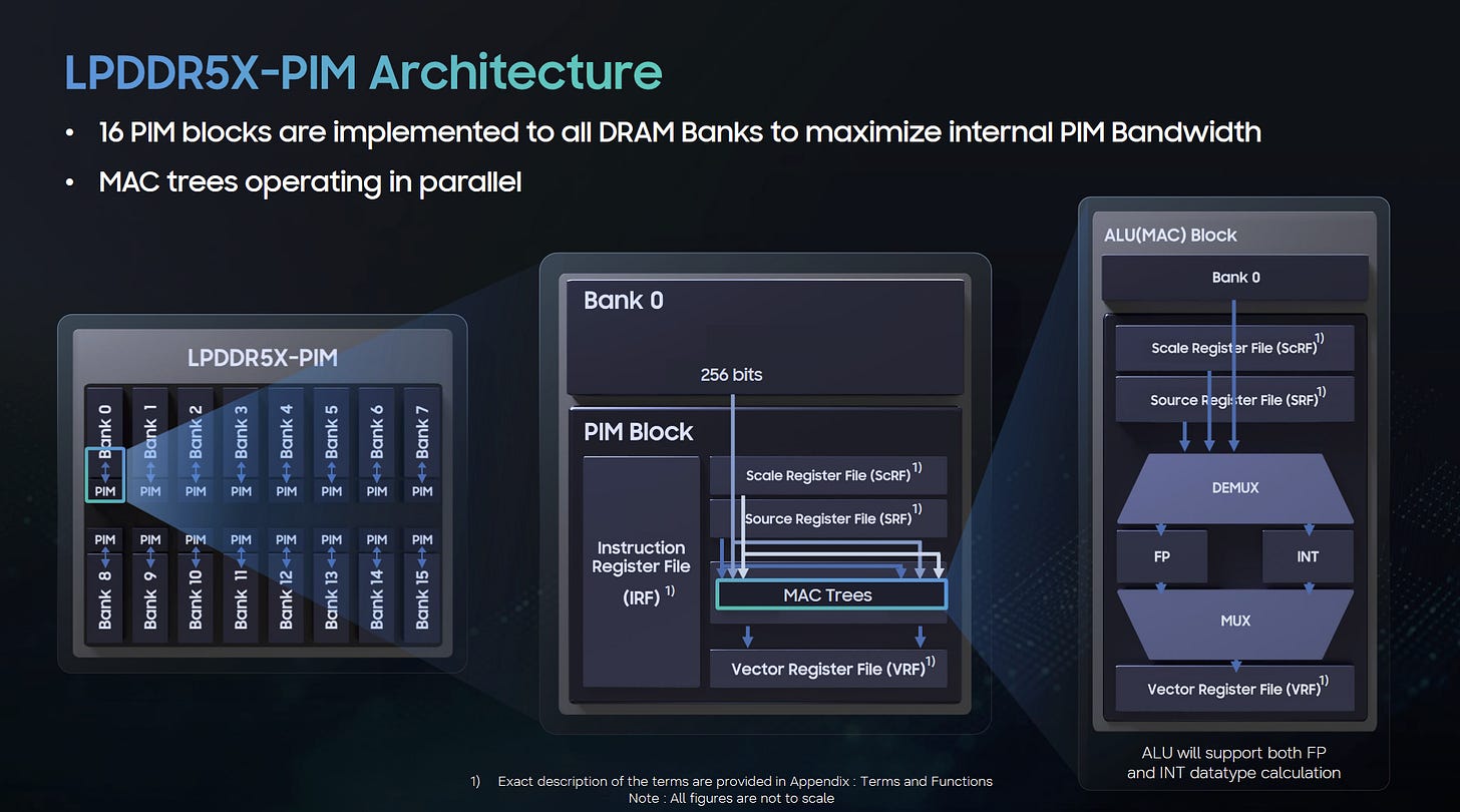
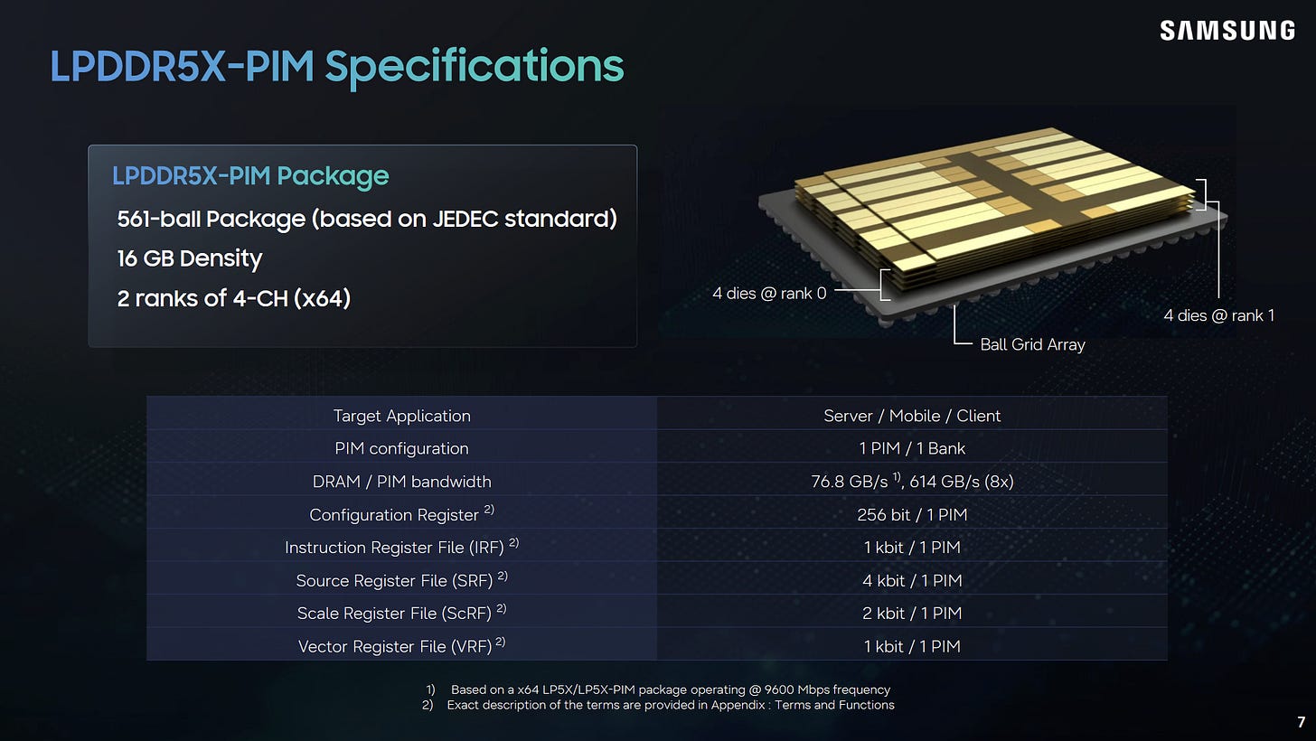
Samsung's LPDDR5X-PIM (based on the LPDDR5X-9600 spec) features 16 banks, but with a critical addition: a PIM block is attached to every single bank. These blocks operate independently of the external bus, allowing them to tap into the full internal bandwidth of the chip.
Bandwidth Comparison
| Feature | Standard LPDDR5X | LPDDR5X-PIM |
|---|---|---|
| Parallel Bank Access | Max 2 banks | All 16 banks |
| Peak Bandwidth | ||
| Constraint | External Bus Limited | Internal Bandwidth Optimized |
Inside the PIM Block
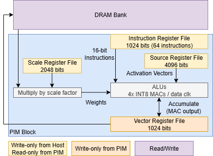
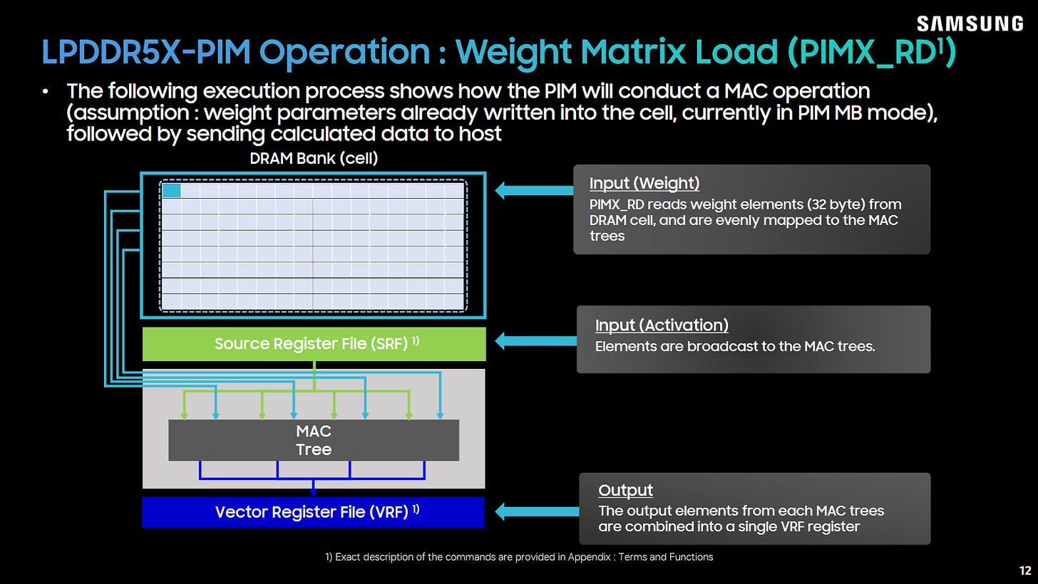
Each PIM block is essentially a specialized compute engine consisting of a MAC (Multiply-Accumulate) tree, control logic, and several register files.
Register Specifications
- Instruction Register File: 1024-bit capacity, storing up to 64 distinct 16-bit instructions.
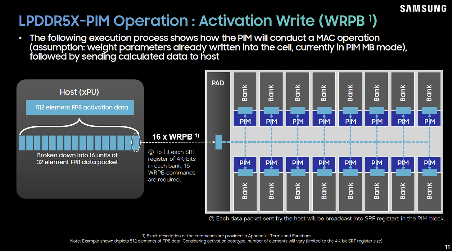
- Source Register File: 4 kbit, used primarily for activation vectors (the first operand).
- Scale Register: 2 kbit, providing scaling factors for the weights.
- DRAM Bank: Supplies the second operand (the model weights).
Compute Performance
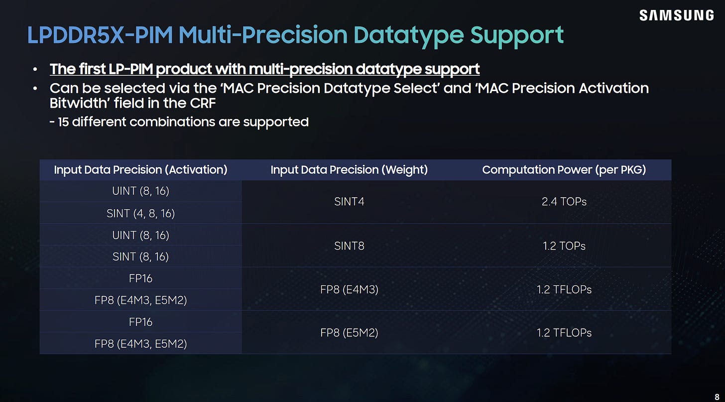
The MAC array is designed for low-precision AI workloads. According to Samsung:
- Standard Throughput: 4 or MAC operations per data clock (which equals 8 per cycle).
- Optimized Throughput: Using 4-bit input weights doubles the performance.
The total compute throughput for a single package is:
While seems modest, scaling is linear. For instance, a system with eight LPDDR5X chips would reach:
Note: This aggregate performance is roughly equivalent to the NPU found in Intel's Meteor Lake. However, this would require of system memory, making it a high-cost configuration.
Interfacing via Standard DDR Commands
A major engineering feat of the LPDDR5X-PIM is that it requires a new memory controller does not require a new memory controller. It remains compatible with the standard LPDDR5X protocol by using "hidden" functionality.
The MMIO Trick
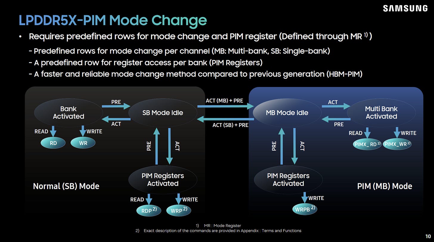
Samsung uses special row addresses that function similarly to Memory-Mapped I/O (MMIO). Activating these specific rows toggles the chip's operating mode:
- Single-Bank Mode: The standard operational mode for normal DRAM access.
- Multi-Bank Mode: Commands are broadcast across all 16 banks simultaneously to maximize internal bandwidth.
- PIM Registers Activated Mode: A state where
READandWRITEcommands target the PIM registers instead of the DRAM cells.
The Execution Workflow
To perform a Machine Learning operation, the software follows this sequence:
- Weight Loading: Load model weights into DRAM using Single-Bank Mode.
- Mode Switch: Transition to Multi-Bank Mode and activate PIM Registers Activated Mode.
- Priming: Write activation values, scale factors, and instructions into the PIM registers.
- Computation: Issue
READcommands. Instead of returning data, these trigger the MAC units to compute and store results in the Vector Register Files (VRF). - Storage: Issue
WRITEcommands to move VRF results back into the DRAM banks. - Retrieval: Switch back to Single-Bank Mode to read the final results as standard data.
Handling Memory Controller Reordering
Because the PIM block expects instructions to access source registers sequentially, a standard memory controller's tendency to reorder accesses would break the logic.
To solve this, Samsung implemented Address Align Mode (AAM). In AAM, the PIM block does not rely on a sequence; instead, it infers the source register index directly from the column address being accessed. This ensures that even if the controller reorders the requests, the correct data is paired with the correct instruction.
Visual References