Diamond Transistor
The Diamond Transistor: A New Era of Semiconductors
In a strategic collaboration with Stanford University, Diamond Foundry is pioneering the development of transistors that utilize diamond as the primary semiconductor material. These ALL-DIAMOND MOSFETs are engineered to achieve switching speeds approximately 50x faster than current standards.
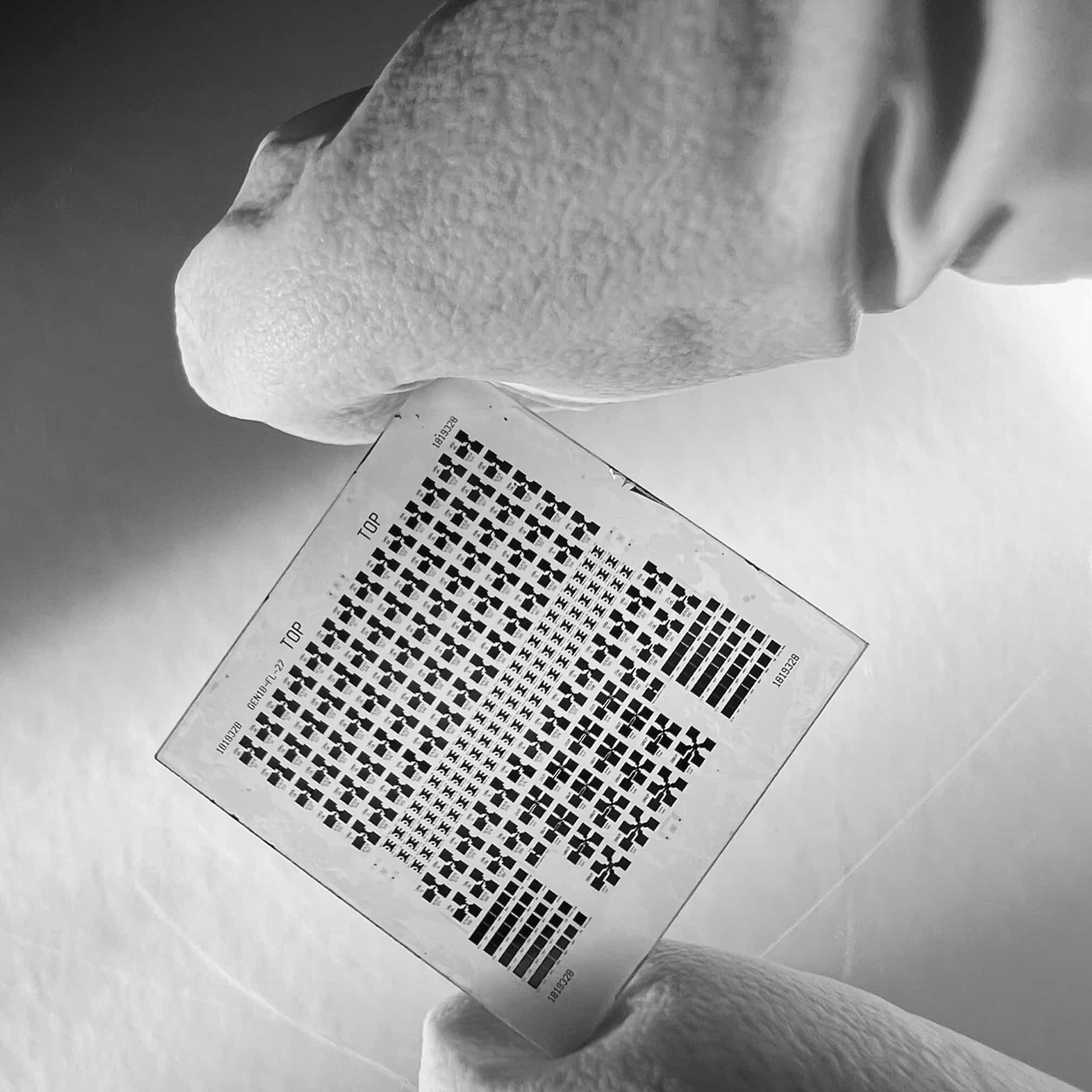
The Innovation: Surface Transfer Doping
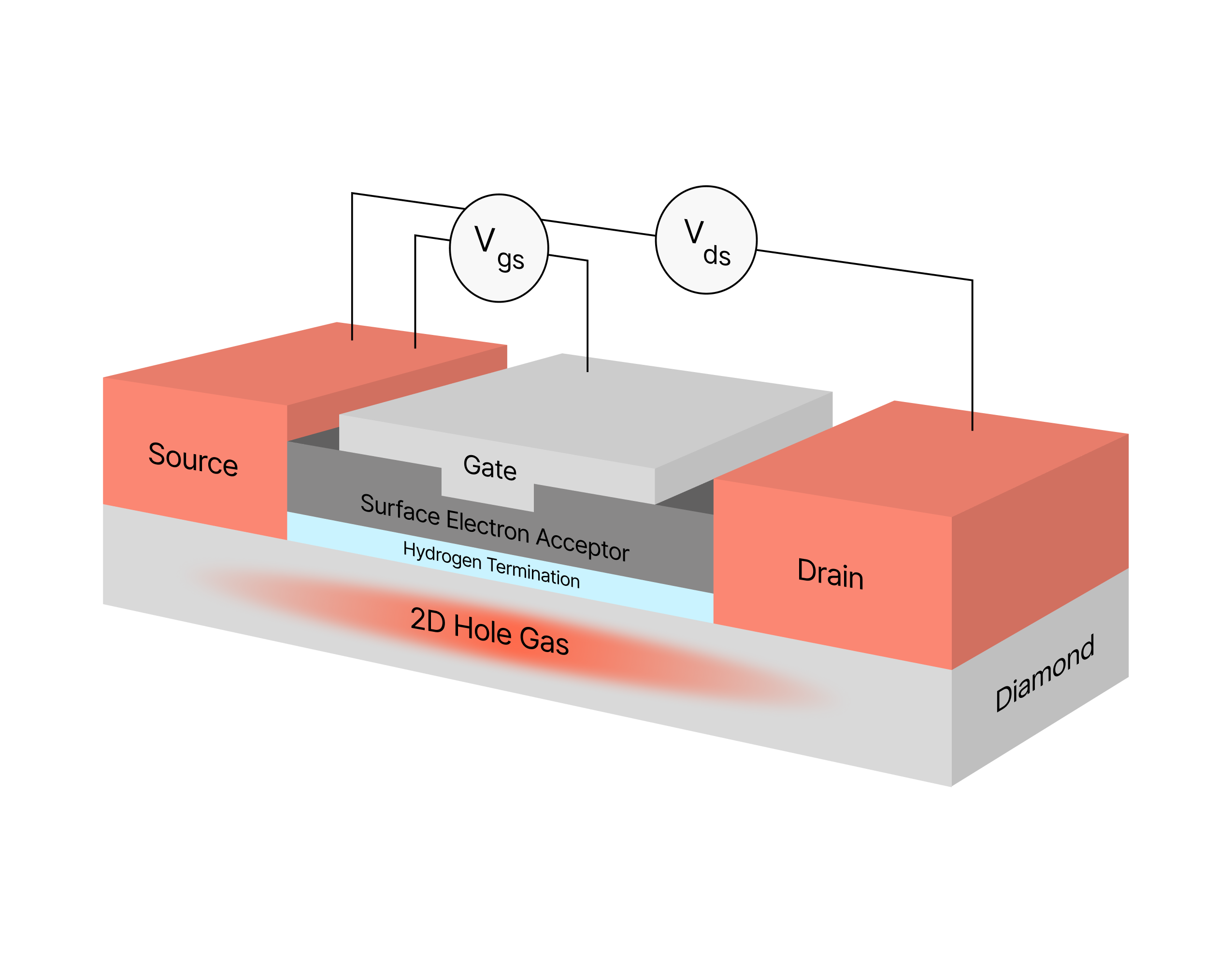
Unlike traditional semiconductor fabrication, these devices utilize surface transfer doping. This method allows for the induction of charge carriers without the need for substitutional dopant atoms to be embedded into the bulk crystal.
How it Works: The Physics
As detailed in the DF Paper in IEEE: On the Conduction Mechanism in Diamond 2-Dimensional Hole Gas Field Effect Transistors:
When the surface of a single-crystal diamond wafer is terminated with an atomic layer of hydrogen, its electron affinity becomes negative. This allows electrons to migrate from the diamond valence band to suitable acceptor species (such as engineered surface layers or adsorbates) located at the surface.
Mathematically, this shift in electron affinity enables the transition:
This process results in the creation of a high-density 2DHG (two-dimensional hole gas) restricted to a few nanometers from the surface. This creates p-type conductivity while maintaining the diamond's:
- Intrinsic Purity
- Thermal Conductivity
- Breakdown Strength
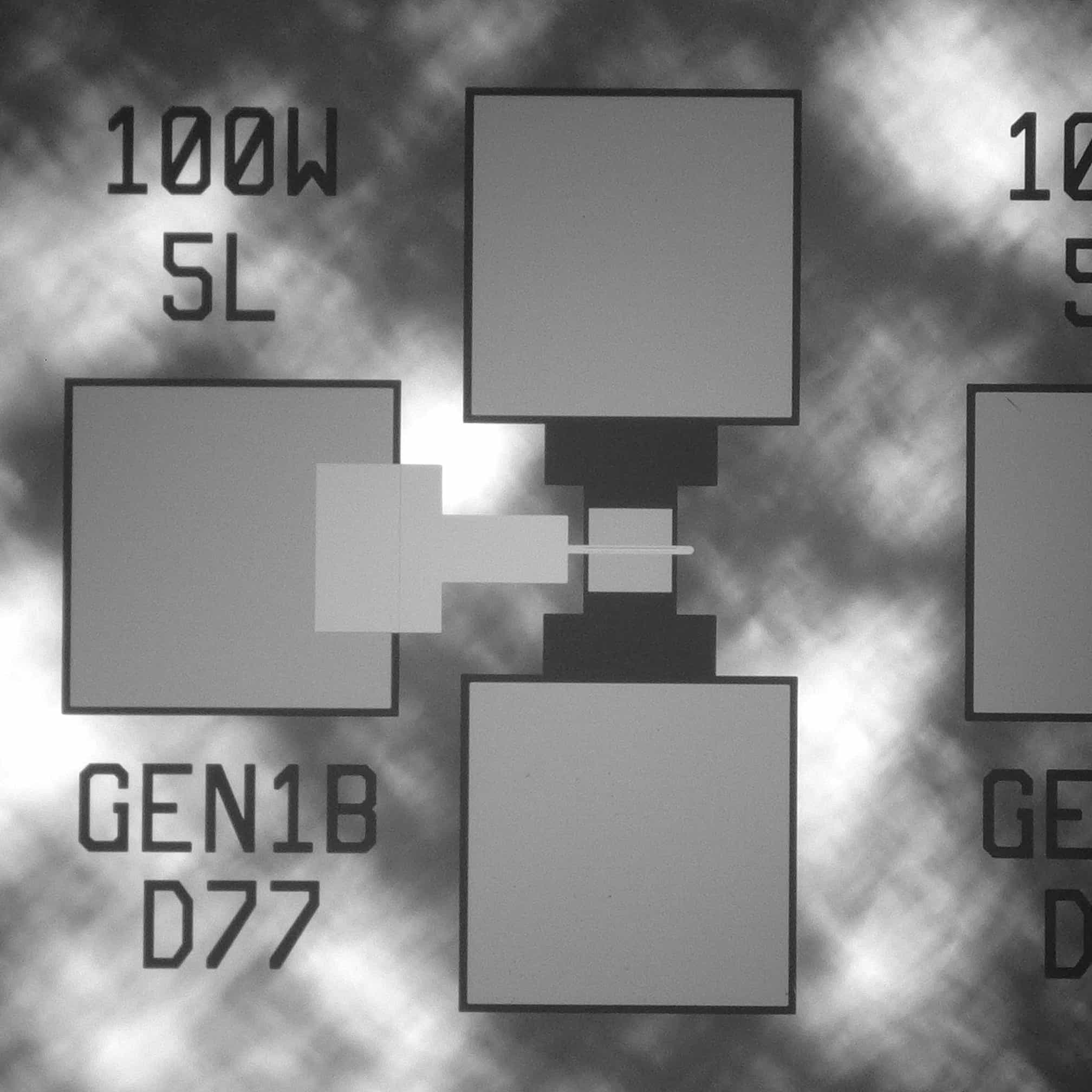
Process Flow
Performance and Applications
By eliminating ion implantation and lattice substitution, Diamond Foundry avoids the carrier scattering and defect generation typical of conventional doping. This makes the technology ideal for:
- High-Power Electronics
- High-Frequency Systems
- Radiation-Hardened Platforms
Benchmarking against Silicon
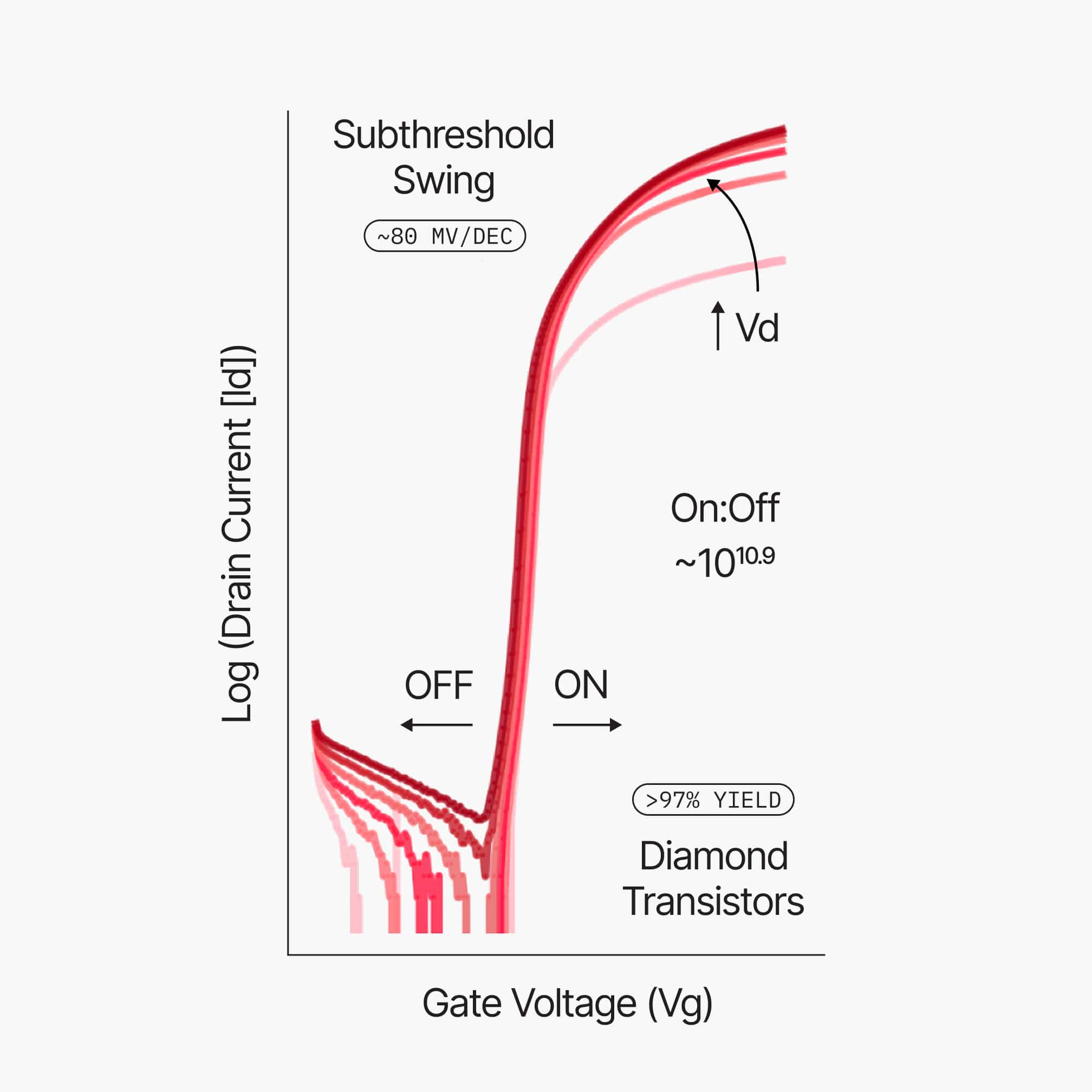
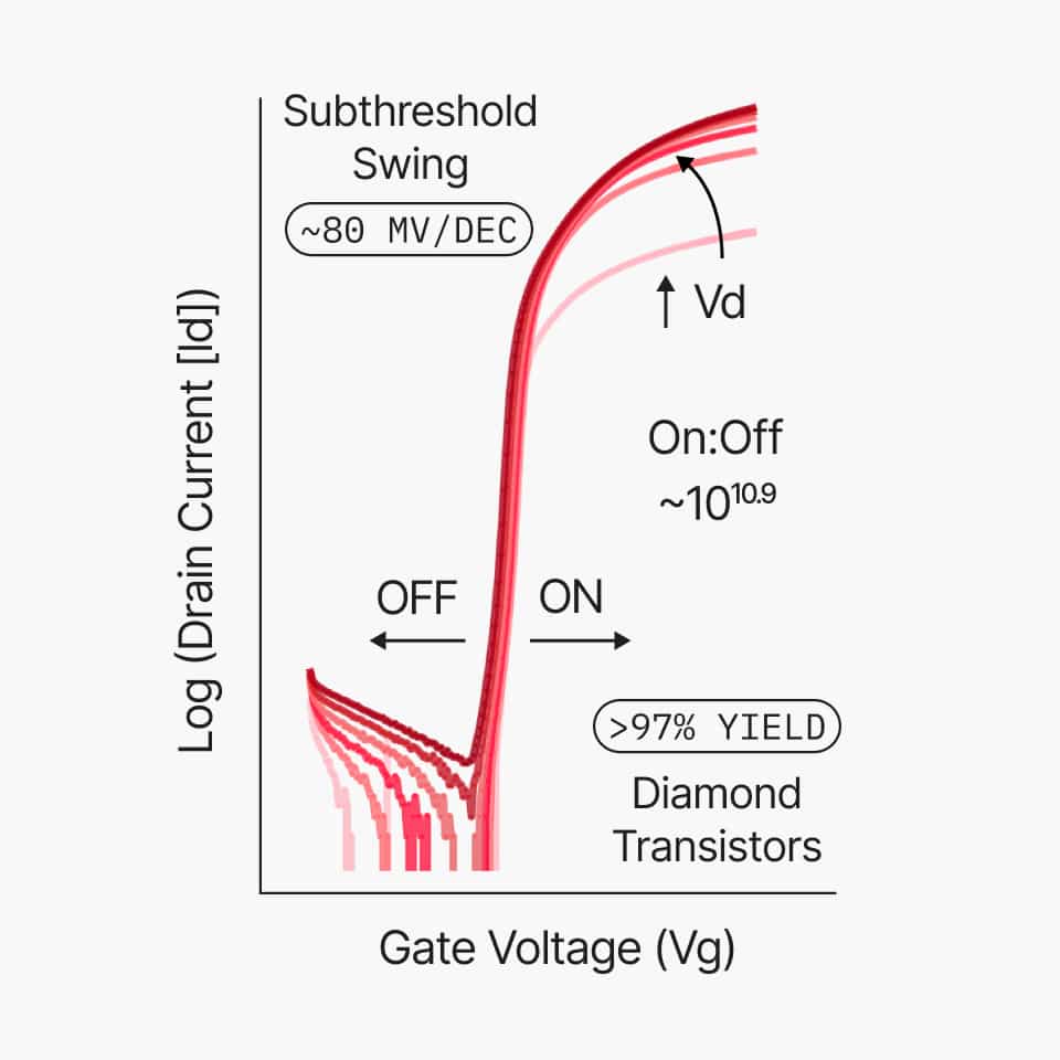
DF's current devices have reached a milestone in efficiency, specifically regarding the subthreshold swing.
| Feature | Traditional 3nm Silicon | DF Diamond Transistor |
|---|---|---|
| Subthreshold Swing | State-of-the-art | Matching Performance |
| Switching Speed | Standard | Faster |
| Doping Method | Substitutional | Surface Transfer |
Ecosystem and Roadmap
Diamond Foundry provides the essential diamond substrates to various R&D organizations currently building the next generation of diamond-based transistors.
Navigation & Resources
- Explore Substrates
- Review DF Tech Stack
- Analyze DF Operations
- Read DF Insights
Company Milestones
The following timeline highlights recent breakthroughs and expansions:
- Nov 25, 2025: Expansion of manufacturing with a new $2.77B fab located in Spain.
- Nov 4, 2023: Featured in the Wall Street Journal regarding diamond's role in accelerating microchips.
- Oct 2, 2023: Announcement of the world's first single-crystal diamond wafer.
{
  "company": "Diamond Foundry",
  "product": "Diamond Transistor",
  "key_metric": "50x switching speed",
  "partnership": "Stanford University"
}